Intro
Although it looks slightly overkill, the idea behind this design was to check if my NoC (Network-on-chip) RTL would work into a real hardware “FPGA”. Then some weeks ago, during my summer holidays, I decided to put some effort into that, without any fancy approach but using a well-known RV core and my largest FPGA. So far till that moment, the only confirmation that the design was working as it’s supposed to be, was through some python tests that were implemented to cover different aspects. Here below there is a resume of my short journey of implementing this MPSoC design.
The components
To compose the design, I wouldn’t want to use anything proprietary or platform-dependent, such as Xilinx/Altera IPs, my main target was to design it all with open source Github based components. Furthermore, I was planning to use an open-source simulation tool like Verilator once if any user wants to try it out, no vendor thing would block from doing it. My only tool exception was to target my largest FPGA synthesis, where I’ve used Vivado to synthesize the design. It was in the queue to test how it’d be with Symbiflow/Project x-ray, however as I wasn’t planning to spend an amount of time on this, I’ve decided by the simple way IMO.
The tiles
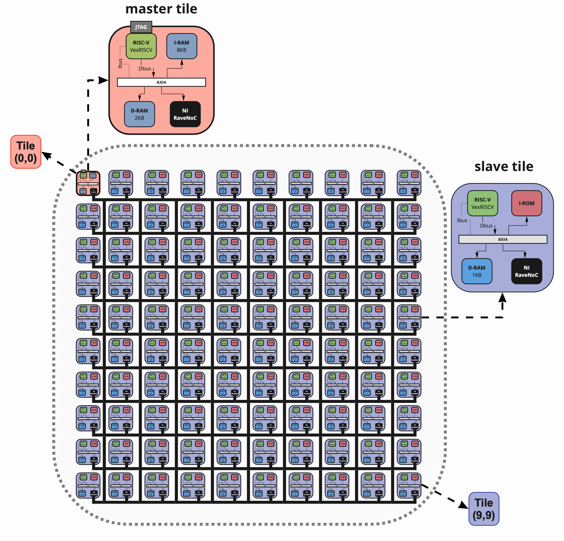
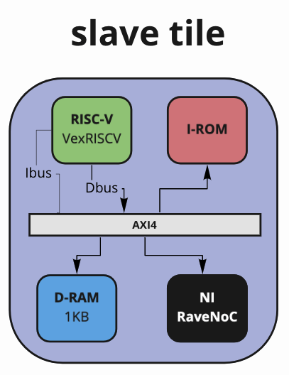
For this project, the first idea I had was the one I stayed with, so I had in my mind: build two tiles, one slave and one master and replicate it many times. With the master tile having a bit more stuff like JTAG and a larger data RAM. Also instead of having an Instruction RAM, I decided to use a boot ROM for the slave tiles with a simple program to answer master calls through the NoC. Again, nothing fancy just to see if I could request from the master to all slaves in the network. For the slave tile, I defined the following components:
- AXI4 interconnect bus
- AXI4 memory
- VexRISCV core (smallest cfg) with some tweaks to enable AXI4 and mtvec[RW] - RV32I
- AXI4 NI Network-Interface with RaveNoC
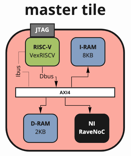
Well, not that different for the master tile this is what I chose:
- AXI4 interconnect bus
- AXI4 memory
- VexRISCV core (simple cfg) mult/div extension, full barrel shifter and has JTAG
- AXI4 NI Network-Interface with RaveNoC
So that was all, pretty much straightforward hardware, nothing custom or different from what’s already available on the web. With all that in place, I just encapsulated the NoC in the top and have added the generates, having in the end, a smaller top which has listed all the modules and instantiates a configurable number of tiles depending upon NoC size/cfg. With the design ready, it was time to get some waves to check if everything was moving in a good direction.
The final design with all modules with a 9x9 RaveNoC is the following one:

Simulation
For the simulation, as I had tried in the past, Verilator was my best choice, once it’s open-source and easy to write testbenches in cpp. Quickly copying and pasting from my previous personal projects, my tb has nothing but the dut instantiation and a modified version of my ELF loader, which I was using at first to test boot ROM of slave tiles. Later on, I changed to only load the ELF into the master tile once the boot ROM on the slaves was working as it suppose to. To enable my cpp ELF loader to write into the memories, I implemented the functions below at the top of the tiles calling these in the tb at sim #t0.
// synthesis translate_off
  function automatic void writeWordIRAM(addr_val, word_val);
    /* verilator public */
    logic [31:0] addr_val;
    logic [31:0] word_val;
    u_ram_instr_rv.u_ram.mem[addr_val] = word_val;
  endfunction

  function automatic void writeWordDRAM(addr_val, word_val);
    /* verilator public */
    logic [31:0] addr_val;
    logic [31:0] word_val;
    //u_ram_rv.u_ram.mem[addr_val] = word_val;
  endfunction
  // synthesis translate_on
It’s considerable to mention that the comment "// synthesis translate_on/off" was there to force Vivado to ignore these constructions when implementing. Technically that’s not required because it’s going to do that anyway although if you have hierarchical mention of the memory arrays like I do there, the tool will not infer BRAMs, creating memories with LUTs what means that you’re 1-wasting FPGA resources and 2-increasing the size of your design once it will consume a lot of logic slices for that.
My first attempt to communicate with the slaves through the NoC wasn’t that good, I have forgotten to change mtvec CSR to point to the location where it was declared my external IRQ function. Thankfully after two/three cups of coffee, I was able to see the obvious in the sims. Since the beginning, I didn’t want to code a complex handshake, so what I decided to do was to implement the following protocol between the single master and the 99x slaves:
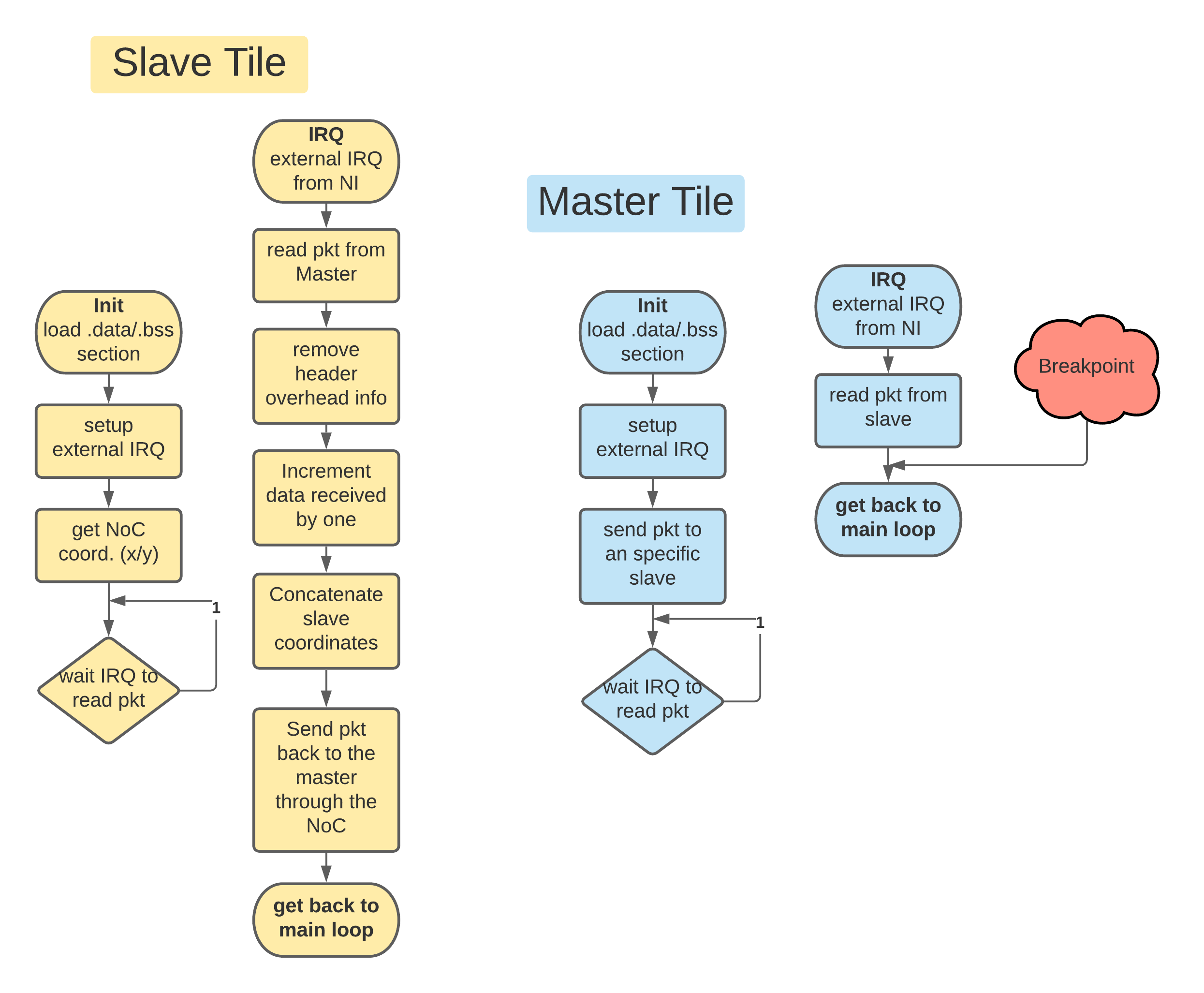
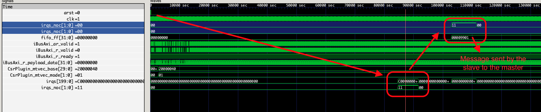
As the master tile has a JTAG interface I could easily switch from one slave coordinates to another without any worries, once it was as easy as compiling it again and loading through the I/F in the FPGA or through an ELF loader in my tb. With the boot ROM working and the master sending the packets correctly in the NoC, I saw it working after some runs. In the image below you can see the design being released from the reset, then the last slave in the NoC [aka x=9/y=9] receives an IRQ, reads the packet, operates on it, and sends it back to the master with the payload modified.

Verilator hint for medium/large designs
I guess worth it to explain here something I have done to speed up the verilation (process to convert from Verilog/RTL to cpp classes) when playing with my sims. When building something that can be considered a medium size design, the tool might take ages to run all the steps into conversion so I found something useful in the Verilator’s FAQ. This a way to indicate to Verilator that you have a design that’s repeated many times and it can be processed into an hierarchical way or something like that. In my case, it changed from 120+ mins to 15 mins worst case. One of the drawbacks is that you need to remember to change the configuration file every time you change the wrapper name where is encapsulated the repetitive design because the output error seems a bit odd and it doesn’t explain to you explicitly why it’s failing to build (was almost mad when I discovered that xD). Another disadvantage is that you lose visibility of your structs and nested modules, although I suppose when you are building something like that, you pretty much already know what’s going on inside there.
The design and the FPGA
When I first saw it working on sims, I was pretty much confident it’d work straight away on the FPGA once I wasn’t adding any MMCM, clock generators, or anything vendor/part-number specific. However, I didn’t start with 100x cores in my first synth and I knew that would fit in my board, unfortunately, I don’t have a crystal ball. So I started with an 8x8 design and discovered that my NoC with 2x flits buffer was consuming a considerable amount of the whole design LUT space. And my FPGA is a Kintex 7 - xc7k325tffg676-2 which has around >203k LUT in total.
Having an easily configurable NoC was the advantage on playing with the parameters to see how big I could increase my design and/or shrink some internal buffers. After several tries and decreasing my initial VexRISCV core parameters to the smallest possible option I could synthesize with 100x RISC-V cores running @ 100MHz. Again, the initial idea wasn’t to push 100% utilization but if it’s easy to change and it’s interesting to know, why not?!. My final hierarchical report by area utilization was this one in the end.
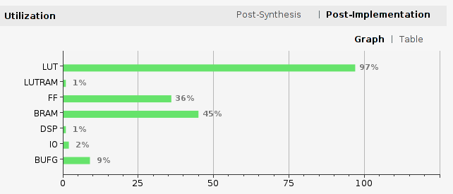
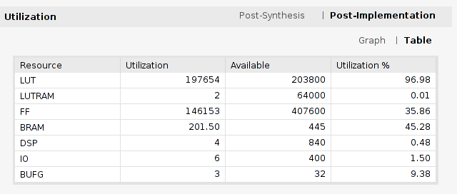
In the end, I had only 3% LUT space left! Still would fit another VexRISCV with steroids, but I was too lazy to try that, maybe another time. The whole congestion/timing in the design wasn’t much awful, as I was running in a low clock freq. for this PN (@100MHz).
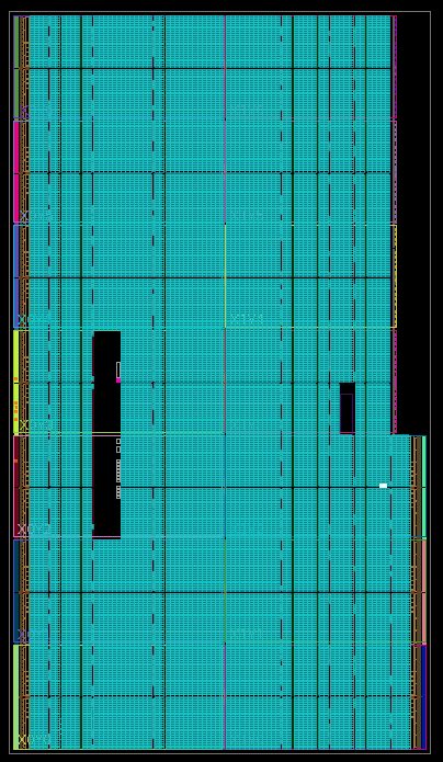 As you can see in the image above, almost every logical slice has something placed, let’s give some thumbs up to Xilinx’s tools at least. xD
FuseSoC
My main source of headaches when dealing with vendor’s tools is to call TCL scripts and face a heterogeneous set of issues about wrong setup, missing files, and a bunch of other “waste of time” stuff. I don’t remember well but most likely that was my motivation when I started looking for a replacement solution. Thankfully there’re impressive engineers such as Olof which started developing some years ago a python package tool called FuseSoC that works as a mixer i.e it takes all your old past frustrations with FPGA vendors + your disruptive RTLs and your ctrl+c/v constraints file and builds for you a bitstream.
Eventually, when it finishes it’ll also try to program your device magically, it’s fantastic and worth giving a try if you never saw it before. Your only duty as a user is to create a YAML core config file that will list all your RTLs/constraints/PN and point that to the tool. Of course, it’s implicit you need to have the vendor tool installed for your FPGA, although it’s magic, the hocus pocus about a license is still required if you’re in Xilinx/Altera’s world. If you’re willing to build this MPSoC for your FPGA, just be careful when launching a run once it takes some time to finish it…

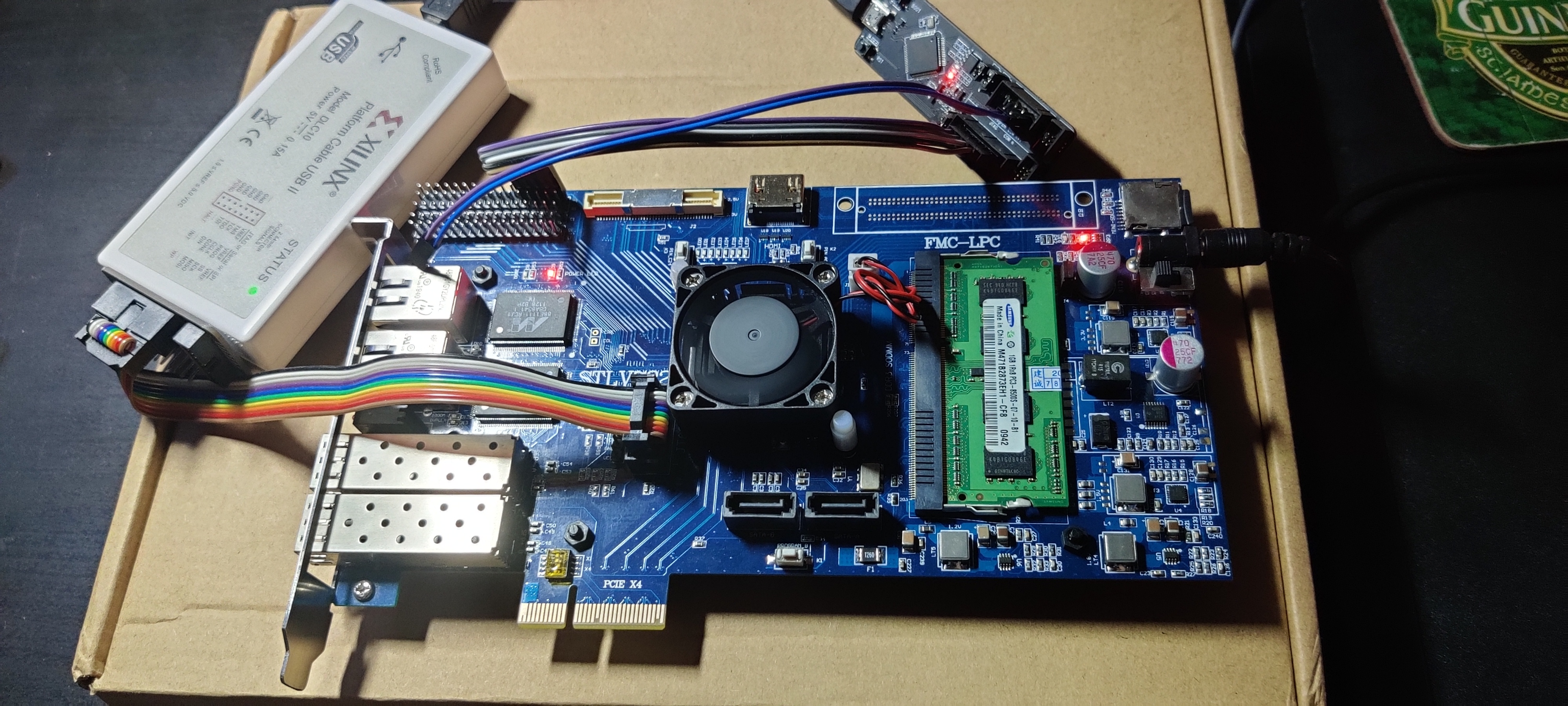
Debugging with real-hardware
After programming the 10.2MB bitstream in the FPGA through Vivado (need to try through open FPGA loader) and connecting the JTAG adapter in the headers, it was time for debugging the program with a real emulation. One of the advantages of using VexRISCV is that the debug module is easy to use and it implements methods to access the busses of the core and put breakpoints/watchpoints all over your SW. For the use with my design, I just downloaded and built their openocd version and in no time was able to start debugging.
To connect the jtag adapter with openocd and start the gdb server:
$ mpsoc_example/sw/openocd_vexriscv -f mpsoc_example/sw/esp-prog.cfg -c "set MPSOC /home/aignacio/mpsoc_example/sw/cpu0.yaml" -f mpsoc_example/sw/mpsoc.cfg
And to launch gdb connecting to the server and sending the ELF file:
$ riscv64-unknown-elf-gdb output/tile_master.elf -ex "target remote localhost:3333" -ex "load"
With the gdb session opened, I just set a breakpoint at the IRQ after reading the RX NI buffer of NoC to see what was the returned packet content.
(gdb) b main.c:47
(gdb) c #Run till bp
(gdb) p/x buffer #print in hex the buffer value
…finally here’s my debug session with the results when talking with the FPGA
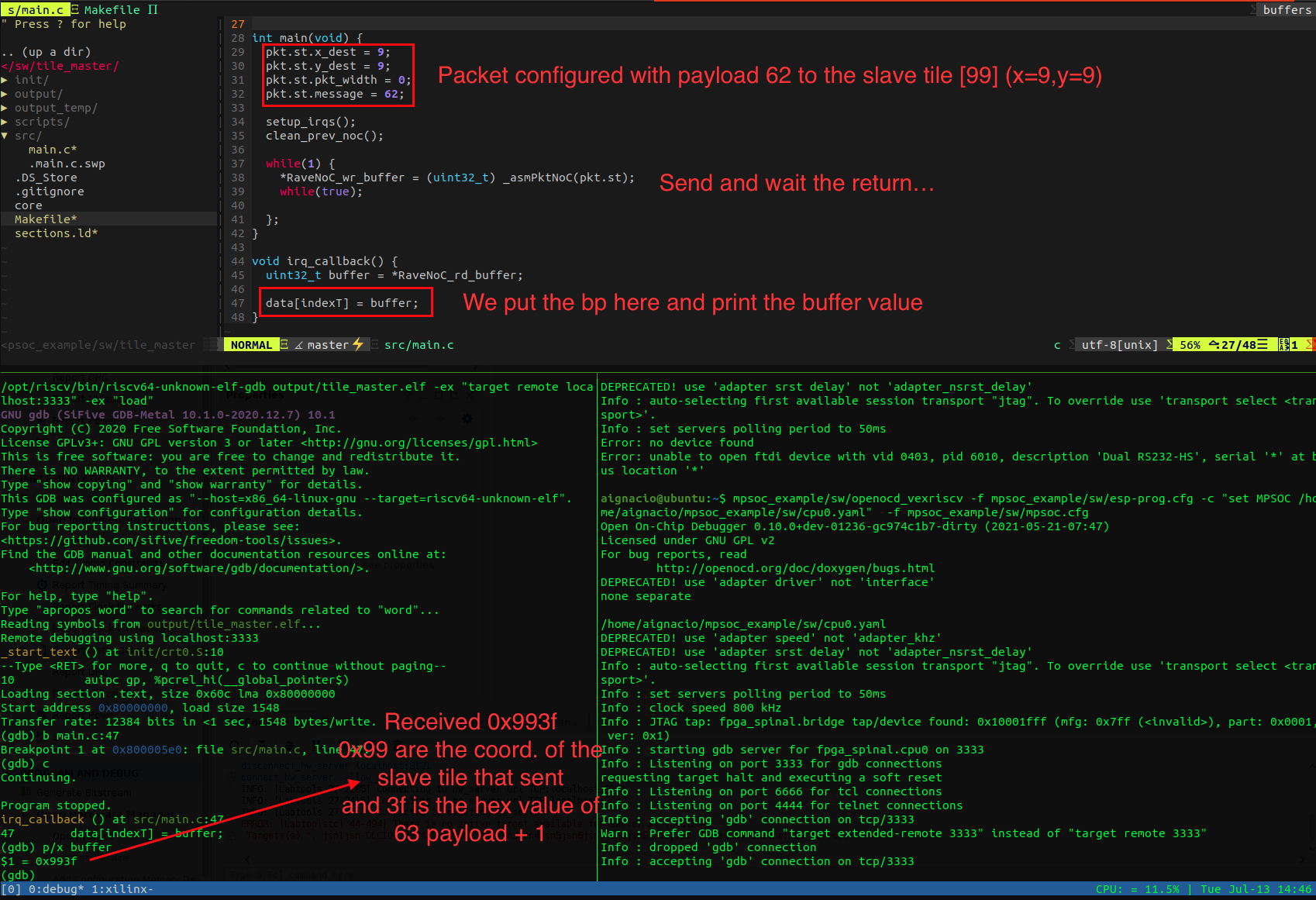 As it can be seen, the last slave tile answers properly as it is supposed to be. I also tried with different slaves and had the same results changing of course the source X/Y in the payload, all operating as they should.
To have access to the design, FuseSoC configuration file, sims, and testbench, please check this repository.